 English
 Español
 Deutsch
-

Deep drawing mold for front and rear wheels of two-wheeled electric vehicles
This Deep drawing mold for front and rear wheels o...
-
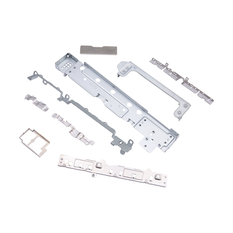
Small stamped parts for laptops and mobile phones
As essential internal components for modern portab...
-
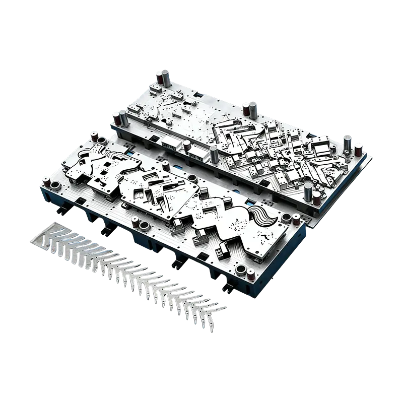
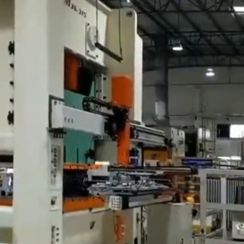
Progressive molds for automotive parts
This Continuous mold for automotive motor housing ...
-
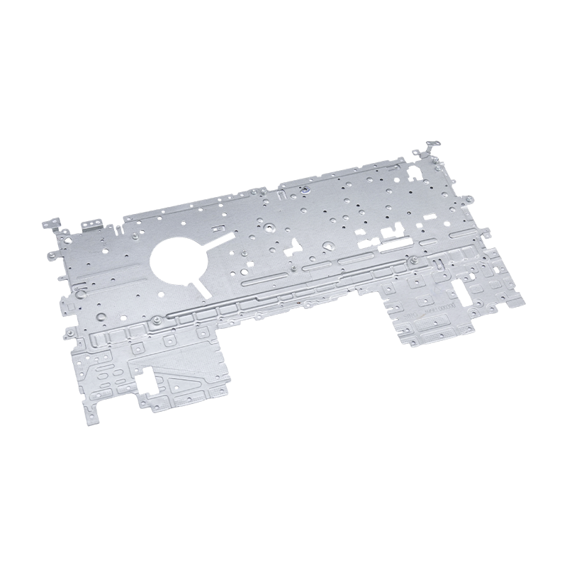
Laptop stamping parts
Our laptop stamping parts are precision-manufactur...
-
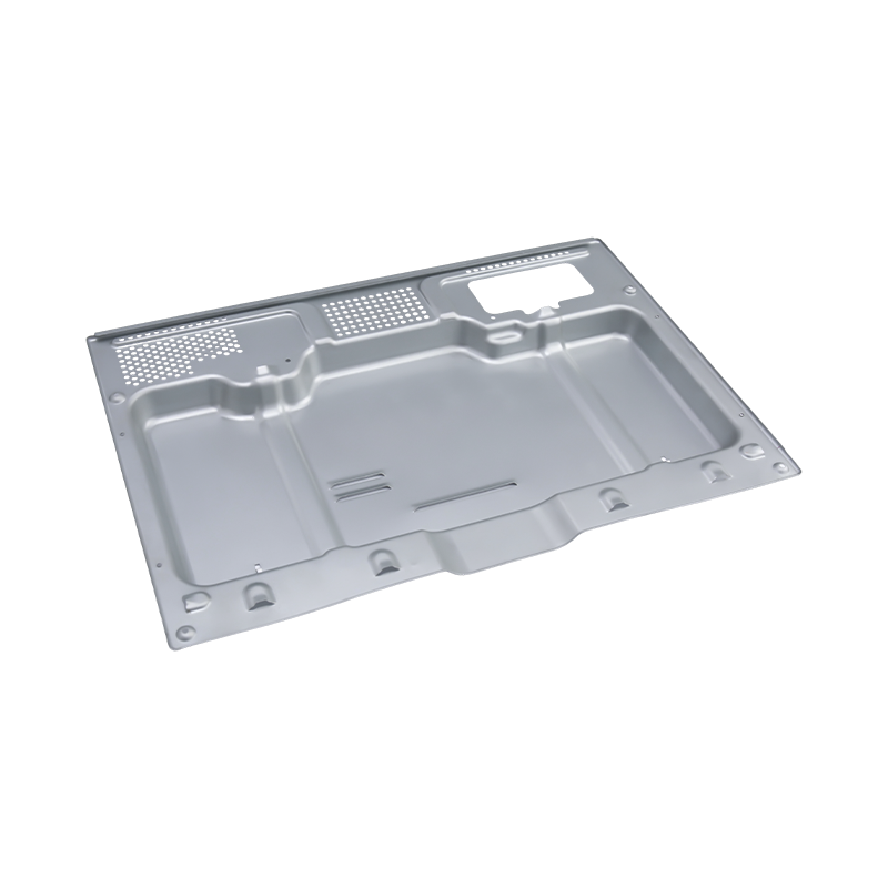
High-end oven stamping parts
Our High-end oven stamping parts are precision-man...
- E-mail us: [email protected]
- Call us: +86-139 1308 8972
Industry News
Home / News / Industry News / What Are the Key Differences Between Micro-Stamping and Standard Electronic Parts?
What Are the Key Differences Between Micro-Stamping and Standard Electronic Parts?
2026-03-09
Content
- 1 Understanding Electronic Stamping Parts and Their Role in Modern Electronics
- 2 Defining Standard Electronic Stamping Parts: Dimensions and Capabilities
- 3 What Defines Micro-Stamping and Where It Diverges From Standard Practice
- 4 Tooling Design and Die Construction: Where the Differences Are Most Pronounced
- 5 Press Equipment and Process Control Requirements
- 6 Side-by-Side Comparison of Key Characteristics
- 7 Material Selection Differences for Micro-Scale Electronic Stamping Parts
- 8 Quality Inspection and Measurement Challenges at Micro Scale
- 9 Choosing Between Micro and Standard Electronic Stamping Parts for Your Application
Understanding Electronic Stamping Parts and Their Role in Modern Electronics
Electronic stamping parts are precision metal components manufactured through a progressive or transfer stamping process in which flat metal sheet or coil stock is progressively formed, punched, bent, and shaped by hardened die sets to produce finished parts with tight dimensional tolerances. These components form the structural and electrical foundation of virtually every electronic device in production today — from consumer smartphones and laptops to automotive control modules, medical implants, and industrial sensors. The category encompasses an enormous variety of component types including terminals, connectors, shields, brackets, contacts, lead frames, heat spreaders, and spring elements, all sharing the common characteristic of being formed from metal sheet rather than machined from solid stock or cast from molten metal. Within the broad universe of electronic stamping parts, the distinction between micro-stamping and standard stamping represents one of the most practically significant dividing lines in manufacturing capability, process requirements, and end-use application suitability.
Defining Standard Electronic Stamping Parts: Dimensions and Capabilities
Standard electronic stamping parts occupy the broad middle ground of the stamping industry, encompassing components with feature sizes and material thicknesses that conventional progressive die tooling and standard stamping presses can reliably produce at high volume. In practical terms, standard electronic stamping parts are typically produced from sheet metal with thicknesses ranging from approximately 0.15 mm to 3.0 mm, with punched holes, formed features, and bend radii that are dimensioned in tenths of a millimetre rather than microns. Dimensional tolerances on standard electronic stamping parts generally fall in the range of ±0.05 mm to ±0.1 mm, achievable with well-maintained conventional tooling on press equipment ranging from 25-tonne bench-top units to 400-tonne transfer presses for larger components.
The material range for standard electronic stamping parts is broad and includes cold-rolled steel, stainless steel grades 301 and 304, copper alloys such as C110, C194, and C260 brass, aluminium alloys 1100 and 3003, and nickel silver. Surface finishing options including electroplating with tin, nickel, silver, or gold are routinely applied to standard electronic stamping parts to achieve the contact resistance, corrosion resistance, and solderability characteristics required for their specific circuit or mechanical function. Production volumes for standard electronic stamping parts can range from thousands to hundreds of millions of pieces per year, with progressive die tooling enabling cycle rates of 100 to 800 strokes per minute depending on part complexity and press size.
What Defines Micro-Stamping and Where It Diverges From Standard Practice
Micro-stamping enters the picture when the dimensional requirements of electronic stamping parts exceed what standard tooling and process controls can reliably deliver. While there is no universally agreed threshold, micro-stamping is generally understood to begin when material thickness falls below 0.1 mm, when punched feature sizes approach or exceed a ratio of 1:1 with the material thickness (meaning hole diameters equal to or smaller than the sheet thickness being punched), or when overall part dimensions are measured in single-digit millimetres with tolerances tightened to ±0.005 mm to ±0.02 mm. At this scale, the physical laws governing metal deformation, tool wear, and press dynamics require fundamentally different approaches to die design, press selection, process control, and quality inspection compared to standard electronic stamping parts production.
The electronics industry's relentless drive toward miniaturisation is the primary force expanding the market for micro-stamped electronic stamping parts. Smartphone connectors, hearing aid components, wearable sensor housings, cardiac pacemaker lead contacts, MEMS device packaging, and fine-pitch IC lead frames all demand micro-stamped features that simply cannot be produced to specification using conventional stamping approaches. The gap between what standard and micro-stamping can achieve has grown wider as device miniaturisation has accelerated, making the distinction between these two categories increasingly commercially and technically significant.
Tooling Design and Die Construction: Where the Differences Are Most Pronounced
The die tooling used to produce micro-stamped electronic stamping parts differs from standard tooling in almost every aspect of its design, material specification, and manufacturing process. Standard progressive dies for electronic stamping parts are constructed from tool steel grades such as D2, M2, or DC53, with punch and die clearances typically set at 5–10% of material thickness per side. At standard dimensions, these clearances are achievable with conventional CNC grinding and EDM wire cutting equipment, and the resulting tools can produce millions of parts before requiring reconditioning.
Micro-stamping dies for miniature electronic stamping parts require clearances measured in single-digit microns — sometimes as little as 1–3 microns per side for the finest features — demanding die components manufactured on ultra-precision grinding machines and profile EDM equipment capable of holding tolerances of ±0.001 mm or better. Punch diameters for micro-stamped features can be as small as 0.05 mm, at which scale the punch is mechanically fragile and susceptible to deflection under the lateral forces generated during punching. Die designers compensate through guide bush arrangements that support the punch close to the cutting face, reduced die entry lengths that minimise the unsupported punch length, and controlled punch-to-die alignment achieved through precision ground guide pillars and bushes with micron-level clearances.
Carbide tooling — specifically tungsten carbide grades selected for their combination of hardness, toughness, and compressive strength — is essentially mandatory for micro-stamped electronic stamping parts production. The wear rate of tool steel at micro-scale punch dimensions would render tooling economically unviable within a short production run. Carbide dies, while significantly more expensive to fabricate than tool steel equivalents, provide the wear resistance and dimensional stability needed to maintain feature size and edge quality across the millions of strokes required for cost-effective micro-stamped electronic stamping parts production.
Press Equipment and Process Control Requirements
The press equipment used for micro-stamped electronic stamping parts differs substantially from standard stamping press specifications. Standard electronic stamping parts production tolerates a degree of press frame deflection, slide parallelism variation, and dynamic vibration that would be catastrophic at micro-scale. Micro-stamping presses are built to substantially tighter slide guidance specifications — typically 0.003 mm or better parallelism — using hydrostatic or precision roller bearing slide guides that maintain consistent shut height regardless of eccentric loading from asymmetric part geometries.
Servo-driven micro-stamping presses offer particular advantages for precision electronic stamping parts production at micro-scale. The ability to program arbitrary slide motion profiles — slow approach to contact for delicate features, rapid return for cycle time optimisation, controlled dwell at bottom dead centre for coining operations — provides a level of process flexibility that crank-driven mechanical presses cannot match. Servo presses also eliminate the energy peaks associated with flywheel-driven mechanical presses, reducing vibration transmitted to the die and improving dimensional consistency across long production runs of micro-stamped electronic stamping parts.
Side-by-Side Comparison of Key Characteristics
The table below provides a structured comparison of the principal differences between micro-stamping and standard processes for electronic stamping parts across the dimensions most relevant to design engineers and procurement specialists:
| Characteristic | Standard Electronic Stamping Parts | Micro-Stamped Electronic Stamping Parts |
| Material thickness range | 0.15 mm – 3.0 mm | 0.01 mm – 0.1 mm |
| Dimensional tolerance | ±0.05 mm – ±0.1 mm | ±0.005 mm – ±0.02 mm |
| Die clearance per side | 5–10% of material thickness | 1–3 microns absolute |
| Tooling material | Tool steel (D2, M2, DC53) | Tungsten carbide |
| Press type | Mechanical / hydraulic | Precision servo / hydrostatic guide |
| Typical stroke rate | 100–800 spm | 200–1,500 spm (servo-optimised) |
| Inspection method | CMM, optical comparator | Vision systems, SEM, confocal microscopy |
| Tooling cost | Moderate | High to very high |
Material Selection Differences for Micro-Scale Electronic Stamping Parts
Material selection for micro-stamped electronic stamping parts involves additional constraints beyond those that apply to standard components. At thicknesses below 0.1 mm, the microstructure of the metal becomes directly relevant to stamping behaviour — grain size relative to material thickness can cause inconsistent deformation, burr formation, and edge quality variation that would be negligible at standard thicknesses. Micro-stamping applications typically specify materials with controlled grain structures, often designated by ASTM or JIS fine-grain specifications, to ensure consistent metal flow and cut edge quality across the stamping operation.
Copper alloys remain the most common conductor materials for micro-stamped electronic stamping parts, particularly C194 (copper-iron-phosphorus) and C7025 (copper-nickel-silicon) grades that offer good electrical conductivity combined with the spring characteristics and formability needed for miniature contact and terminal applications. Beryllium copper alloys, particularly C17200 in the solution-annealed condition, are specified for micro-stamped spring contacts where maximum elastic deflection under load is required, though their processing requires careful attention to health and safety controls during stamping and finishing operations.
Quality Inspection and Measurement Challenges at Micro Scale
Verifying dimensional conformance of micro-stamped electronic stamping parts requires inspection equipment and methodologies that go well beyond the coordinate measuring machines and optical comparators standard in most stamping quality laboratories. Feature sizes measured in tens of microns demand non-contact optical measurement systems — typically automated vision systems with sub-micron resolution objectives and telecentric optics — capable of measuring hundreds of features per part in seconds at production line speeds. For the most critical dimensions, scanning electron microscopy (SEM) provides the resolution needed to characterise edge quality, burr height, and surface condition at a level of detail unattainable with light optics.
Statistical process control for micro-stamped electronic stamping parts must be implemented at a level of rigour that goes beyond the typical SPC programmes applied to standard electronic stamping parts production. Die wear at micro-scale produces dimensional drift rates that can exceed tolerance boundaries within a single production shift rather than over the multi-day production runs typical of standard tooling. Real-time SPC with automated feedback to press parameters — adjusting shut height, feed progression, and lubrication delivery in response to measured dimensional trends — is increasingly standard practice in leading micro-stamping operations serving the precision electronics sector.
Choosing Between Micro and Standard Electronic Stamping Parts for Your Application
The decision between specifying micro-stamped or standard electronic stamping parts should be driven by objective functional requirements rather than by the assumption that tighter tolerances always produce better products. Standard electronic stamping parts are appropriate whenever the application's dimensional, electrical, and mechanical performance requirements can be met within the capability envelope of conventional stamping — and in the majority of electronic assembly applications, they can. The significantly lower tooling cost, broader supplier base, and more straightforward quality management associated with standard electronic stamping parts represent genuine advantages that should not be surrendered without clear functional justification.
Micro-stamping should be specified when miniaturisation is a genuine design driver — when reduced component dimensions enable meaningful improvements in device performance, integration density, or end-user experience that justify the higher tooling investment and more complex supply chain management. Applications including ultra-miniature connectors for implantable medical devices, sub-millimetre spring contacts for wearable sensors, fine-pitch lead frames for advanced IC packages, and precision shielding components for RF-sensitive modules all represent cases where the capabilities of micro-stamped electronic stamping parts deliver functional value that cannot be replicated at standard scale.

Previous Post
Metal Stamping Parts for Automotive and Home Appliances: Processes, Materials and Quality Standards
Next Post
What's the Difference Between Traditional and Simulation-Optimized Automotive Stamping Dies?
Our Products.
Start Your Business with an OEM Manufacturer Right Here!
Provide global customers with complete turn-key solutions
through
innovation!
QUICK LINKS
CONTACT INFO.
-
 +86-139 1308 8972
 -

-
 No. 118 Yexin Road, Wujiang Economic Development Zone, Suzhou, China
Copyright © Suzhou Shuangqisi Mold Equipment Co., Ltd. All Rights Reserved. Custom Stamping Die Metal Stamping Die Manufacturers
